
Warpage Control in Advanced Packaging: The CTE Matching Challenge
Advanced packaging has made semiconductor systems more powerful, denser, and more flexible than ever, but it has also exposed a stubborn mechanical problem that refuses to go away: warpage. As heterogeneous integration pushes more dies, more layers, and more materials into a single package, the question of how those materials expand and contract becomes central to yield, reliability, and manufacturability. At the heart of that problem is coefficient of thermal expansion, or CTE, matching.
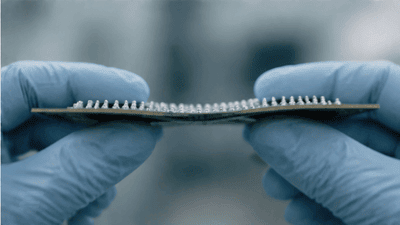
If different materials in a package expand at different rates as temperature changes, the package bends, twists, and distorts. That warpage may be small in absolute terms, but in advanced packaging even tiny deviations can ruin alignment, create assembly defects, or weaken long-term reliability. In many ways, warpage control is the quiet engineering battle underneath the flashy world of chiplets, 3D stacks, fan-out, and AI packages.
Why Warpage Matters So Much Now
In older packages, warpage was a nuisance. In advanced packaging, it is a structural constraint. The reason is simple: modern packages are larger, thinner, and more heterogeneous. They contain silicon dies, organic substrates, interposers, mold compounds, underfills, thermal interfaces, and sometimes stacked memory or 3D structures. Each of these materials responds differently to heat.
Once the package becomes large enough and thin enough, those differences add up. A little mismatch between silicon and organic substrate may be tolerable in a simple package, but in a chiplet module with fine-pitch interconnects, the same mismatch can cause major problems. Micro-bumps may not align correctly, hybrid bonds may fail to meet tolerance, and routing layers may distort enough to reduce assembly yield. In short, warpage is not just a mechanical issue. It is a system-level integration issue.
The CTE Mismatch Problem
CTE describes how much a material expands when temperature rises. Silicon has a relatively low CTE. Many organic substrates, mold compounds, and encapsulants have much higher CTEs. That difference creates stress whenever a package heats up or cools down, which happens constantly during processing, testing, and normal operation.
If two bonded materials expand at different rates, they pull against each other. Over a simple structure, that force may be manageable. Over a large advanced package, it can create significant curvature. The larger the package and the more diverse the materials, the harder it is to keep everything flat. That is why CTE matching is one of the most important design considerations in advanced encapsulation and heterogeneous integration.
The challenge is not to make every material identical. That is impossible. The challenge is to choose materials and structures whose thermal behavior is compatible enough that the package stays within acceptable warpage limits across all operating and assembly conditions.
Where Warpage Shows Up
Warpage can appear at multiple stages of the manufacturing process, and each stage creates its own headaches. During die placement, a warped substrate can make alignment difficult. During reflow or bonding, differential expansion can shift the dies or create local stress. After molding, the package may cool unevenly and lock in residual stress that affects later reliability.
It can show up in:
- Flip-chip assembly, where bump alignment becomes difficult.
- Fan-out packaging, where redistribution layers demand a flat foundation.
- 2.5D interposer-based systems, where large structures must stay planar.
- 3D stacked dies, where the package must tolerate vertical and lateral stress simultaneously.
The problem is especially acute for large AI accelerators and high-bandwidth memory modules. These packages are physically big, thermally intense, and mechanically sensitive. The more functionality gets packed into a single module, the less room there is for error.
Why Advanced Packaging Makes It Harder
Advanced packaging amplifies warpage because it removes the easy margins that existed in older designs. Packages are thinner, interconnect pitch is finer, and die-to-die spacing is tighter. In many cases, designers are also trying to reduce package height and footprint, which leaves less mechanical stiffness to resist bending.
Heterogeneous integration makes the situation more complex because each die or material may have a different thickness, mass, and thermal behavior. A package with a logic die, multiple memory stacks, and an interposer is not just a flat object. It is a layered mechanical system, and every layer affects the others.
This means warpage control must be considered from the start, not patched in at the end. If the package architecture is designed without CTE balance in mind, the resulting warpage may be so severe that no amount of process tuning can fully fix it. That is why packaging teams increasingly co-design mechanical behavior alongside electrical routing and thermal performance.
The Core Strategies for Control
Warpage control in advanced packaging is a multidimensional problem, so there is no single fix. Instead, engineers use a bundle of strategies that work together. Some focus on material choice. Others focus on geometry. Others are process-related. The best results usually come from combining all three.
1. Material Matching
The most obvious approach is to choose materials whose CTE values are closer to one another. If the substrate, mold compound, adhesive, and die stack behave similarly with temperature, the package is less likely to bow. Of course, CTE matching is only one part of the equation, because stiffness, cure shrinkage, and moisture behavior also matter.
Still, material selection is the first line of defense. In some applications, glass-based or silicon-based intermediate structures are used to bridge the thermal gap between silicon dies and more expansive organic materials. That can help reduce stress and improve flatness.
2. Symmetry in Stack-Up
Mechanical symmetry is another powerful tool. If the package stack is balanced top-to-bottom and side-to-side, thermal stress is less likely to cause bending. Uneven die placement, asymmetric copper distribution, or unbalanced molding can all create warpage. Good package design tries to avoid those imbalances wherever possible.
This is one reason advanced package layout has become a serious engineering discipline. Die placement is no longer just about signal routing or thermal hotspots. It is also about how the entire structure will deform under heat.
3. Stiffness Management
A package needs enough stiffness to resist deformation, but not so much that it becomes brittle or difficult to assemble. This balance is tricky. Thicker substrates may reduce warpage, but they may also increase cost or hurt electrical performance. Stronger mold compounds can improve mechanical integrity, but if they are too rigid they may create stress concentration instead of reducing it.
Designers therefore tune the stiffness of each layer to get a package that is strong where it needs to be and compliant where it must absorb stress. Think of it like building a bridge: too flexible and it sags, too rigid and it cracks under load.
4. Process Temperature Control
Because warpage is driven by temperature differences, process control matters a great deal. Bonding, curing, cooling, and reflow all need to be managed carefully. If one side of the package heats faster than the other, or if cooling is uneven, the resulting stress can build in ways that are hard to reverse.
Advanced packaging lines increasingly rely on optimized thermal profiles, controlled ramp rates, and fine-grained process monitoring. The goal is to keep the package within a mechanical window where stress is manageable and the final shape remains close to flat.
5. Temporary Support and Carrier Use
For very thin wafers and delicate packages, temporary carriers can provide mechanical support during processing. This is especially useful in fan-out, wafer thinning, and 3D integration flows. The carrier helps keep the structure flat until the package is stable enough to stand on its own.
That may sound like a simple trick, but it is often crucial. Many advanced packaging problems are not solved by the final design alone. They are solved by what happens during the steps that get the design into the final shape.
Warpage and Heterogeneous Integration
Heterogeneous integration makes warpage control even more important because it combines materials with different thermal and mechanical behavior in one system. A multi-die package may include silicon logic, memory dies, analog chips, passives, and interposers. Some of those elements are thick. Some are thin. Some generate a lot of heat. Others are more fragile. The package has to hold them all together without drifting out of alignment.
This is where the CTE matching challenge becomes a design philosophy rather than a simple materials problem. You are not just matching one material to another. You are balancing an entire ecosystem. The package must stay flat enough for assembly, remain stable enough for reliability, and still perform electrically and thermally at a high level.
In 2.5D systems, the interposer helps distribute signals, but it also introduces another mechanical layer that must be controlled. In 3D stacked systems, the problem becomes even more intense because vertical integration adds thermal gradients and local stress. As packages become more sophisticated, the demand for warpage control only increases.
Measurement and Modeling
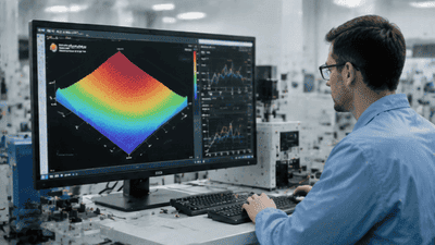
You cannot control what you cannot see, so warpage management depends heavily on measurement and simulation. Package teams use mechanical modeling to predict how a design will behave under thermal load. They also use metrology tools to measure actual curvature, compare it against the model, and refine the design accordingly.
Common tools include:
- Finite element modeling for stress and deformation analysis.
- Optical and laser-based warpage measurement.
- Thermal cycling tests to observe real deformation behavior.
- Correlation studies between predicted and actual package flatness.
This is an iterative process. A package may look acceptable in simulation but perform poorly in practice, or vice versa. The best teams use data from each build to sharpen the next one. That creates a design loop where warpage control steadily improves over time.
Implications for Yield and Reliability
Warpage is not just about assembly convenience. It has direct consequences for yield and reliability. If a package warps too much during assembly, dies may misalign, bonds may fail, or fine-pitch interconnects may be damaged. If warpage persists after assembly, it can weaken solder joints, stress interfaces, and shorten lifetime.
That makes warpage a yield killer in advanced packaging. Even a package that works electrically may be rejected if its shape falls outside the allowable tolerance window. Reliability concerns become even more serious in automotive, aerospace, and industrial applications, where long service life and harsh environments leave very little room for mechanical weakness.
This is why warpage control has become part of product qualification, not just package design. The package must pass both the electrical and mechanical test plan if it is going to ship at scale.
Design Trade-Offs Are Unavoidable
One of the uncomfortable truths in advanced packaging is that perfect warpage control is impossible. Every choice involves trade-offs. A material that reduces warpage may raise cost. A geometry that improves stiffness may hurt electrical routing. A process that limits residual stress may add cycle time or reduce throughput.
That is why warpage management is not about eliminating compromise. It is about choosing the right compromise for the application. A high-end AI package may justify expensive materials and tighter process control if the gain in yield and reliability is large enough. A consumer package may accept a bit more warpage if it keeps cost and throughput under control.
The art of advanced packaging is knowing which compromise the product can afford.
Looking Ahead
As advanced packaging continues to evolve, warpage control will remain one of the defining engineering challenges. New materials, better modeling tools, and improved process control will help, but the underlying physics will not disappear. If anything, the challenge may become more difficult as packages get larger, thinner, and more heterogeneous.
Future developments may include:
- More CTE-compatible substrate and interposer materials.
- Better low-shrink mold compounds for large packages.
- More sophisticated package-level stress compensation.
- Greater use of co-design between electrical and mechanical engineers.
The trend is clear: warpage is moving from a back-end nuisance to a front-end design variable. Teams that address it early will be better positioned to deliver reliable, high-performance heterogeneous systems.
Conclusion
Warpage control in advanced packaging is really the story of CTE matching under pressure. As packages become denser and more heterogeneous, materials that once worked well on their own begin to interact in ways that create mechanical stress, distortion, and yield loss. The challenge is not merely to choose good materials, but to design a complete package ecosystem that stays flat, stable, and reliable across assembly and operation.
That makes warpage one of the most important hidden variables in advanced encapsulation. It affects how well dies align, how reliably bonds form, how long packages survive, and how much the final product costs. In the world of heterogeneous integration, the package is the system, and warpage control is one of the key reasons that system can work at all.





